Introduction
From the LED Lab, we saw that a PN junction is a diode – that is, when a P-type semiconductor contacts an N-type semiconductor. However, it turns out that a metal and a semiconductor can also form a diode, known as a Schottky diode.
Because of the metal-semiconductor junction, Schottky diodes typically have much faster switching and lower forward voltage drop than traditional diodes.
For this lab, gold particles will be evaporated onto the N-type silicon substrate.
Procedure and Results
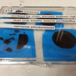
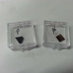
- $N^{+} / N$ epitaxial silicon chips.
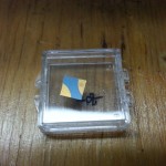
- Silicon chips in their containers.
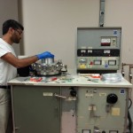
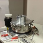
- Vacuum deposition machine.
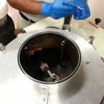
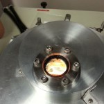
- A small piece of gold foil is placed into a titanium boat.
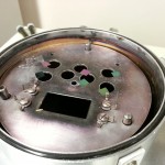
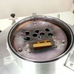
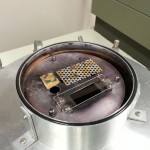
- Chips are laid over holes in the chamber plate.
- Chamber is sealed.
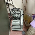
- Vacuum is applied to get the chamber to $< 100 \text{mT}$.
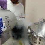
- Liquid $N_2$ is added for the diffusion vacuum to bring the chamber down to $\approx 10 \text{mT}$.
- Current is run through the titanium boat to evaporate the gold.
- A thin layer of gold gets deposited on all exposed surfaces.
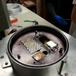
- The chips are flipped upside down and placed on smaller holes for small gold dots.
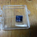
- Both deposition processes complete.
- On the back side, you can see large gold contacts.
- On the front (shiny, $N^{+}$) side, you can see the gold dots that form Schottky junctions with the silicon.
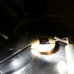
- The chip is placed on the analyzer, and a probe contacts the gold dots.
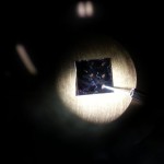
- Close-up of the chip through the microscope.
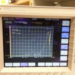
- V-I graph showing that the chip behaves like a schottky diode.
