Introduction
This lab involves the creation of a PN diode. The LED lab already involved the creation of a PN diode, however, the P-type mesas were etched with acid by first coating the layer with a permanent marker, then applying acid to etch away the unmasked material.
This lab will involve the use of industry standard photolithography.
Procedure and Results
-
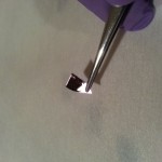
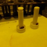
- Obtain a piece of epitaxial silicon.
-
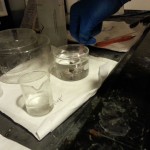
- Put the chips into a boat and dip in DI water, HF, DI water (x2) for an oxide etch.
-
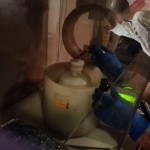
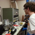
- Place the chips in a field-oxide furnace.
-
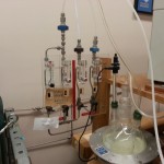
- Oxygen should bubble through water at $1 ft^3/hr$ for 30 minutes at $1100^oC$.
-
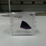
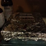
- Cool chips on an aluminum block. Note the color, due to a $\approx 350nm$ thick oxide layer.
-
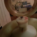
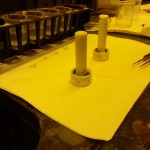
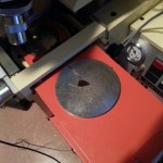
- Place the chip in a centrifuge (with vacuum applied) and add a drop of photoresist.
-
- Turn on the centrifuge to get a very thin photoresist layer.
-
- Place the chips on a hot surface to allow the photoresist to harden.
-
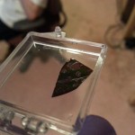
- Chip with smooth layer of photoresist.
-
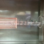
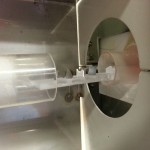
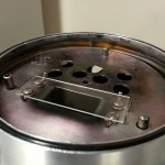
- Place the chip on a UV-expose machine (the mask should just have small dots).
-
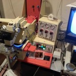
- Make sure the chip is aligned adequately on the mask and apply the UV for 1.5 minutes.
-
- Develop the photoresist (un-exposed regions should dissolve away).
-
- Place the chips on boats and repeat the oxide etch (4 minutes in HF should be enough to remove the thick oxide layer).
-
- Remove the remaining photoresist with acetone, and the oxide holes should be visible.
-
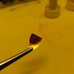
- Place the chips in a boron furnace (note the white boron chips) to P-dope the exposed surfaces. Nitrogen should flow at $1 ft^3/hr$ for 30 minutes at $950^oC$.
-
- Place the chips on an aluminum block to cool.
-
- Warm up the chips on a hot plate.
-
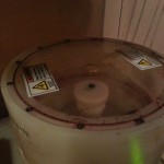
- Place the chips on a centrifuge and clean them by spraying with acetone and isopropyl alcohol.
-
- Apply a drop of photoresist and repeat the centrifuge process, then bake the chips.
-
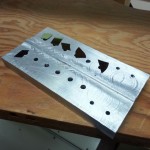
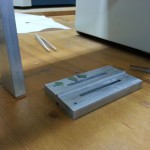
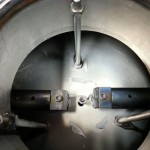
- Contact mask and mask plate.
-
- Place each chip in the UV exposer.
-
- Align the mask to already-existing holes (P-type regions) in the chip.
-
- Expose to UV for 1.5 minutes.
-
- Develop the photoresist.
-
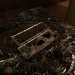
- Result (a little splotchy, but you can see the photoresist regions.
-
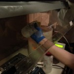
- Load a piece of aluminum into a titanium wire coil.
-
- Place the chips on the vacuum depositor plate.
-
- Deposit aluminum on exposed surfaces. Repeat for the other side of the chips.
-
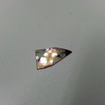
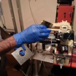
- Peel off aluminum that only coated the photoresist. The result is small aluminum dots over the P-regions.
-
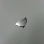
- Back side should be well-covered.
-
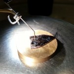
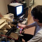
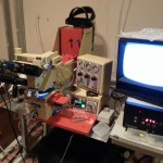
- Place the chip in the analyzer, placing the probe over one of the aluminum dots.
-
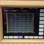
- The V-I curve resembles that of a functioning PN diode.