Introduction
A MOS capacitor is very similar to a Schottky diode except that a thin layer of silicon dioxide is grown before the metal is evaporated. Since the oxide is an insulator, current cannot flow into the device, and there is no IV curve. However, the metal and semiconductor are still coupled through electric fields and thus the voltage can control the charge density at the silicon surface. One characteristic of a MOS capacitor not found in a Schottky diode is an inversion layer.
Two different oxides are made: thin oxides (50nm or so) for MOS capacitors and transistor gates, and thick oxides (400nm or so) for isolation.
Procedure and Results
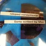
- $N$ doped nonepitaxial silicon chips.
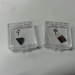
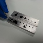
- Silicon chips separated and placed in small boxes.
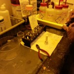
- The chips are put in a boat, then placed in deionized water, then oxide etch for 3 minutes, then two more applications of deionized water.
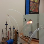
- The chips are loaded into an oxide furnace at $1000^o C$ for 40 minutes (the first 30 minutes are oxygen; the last 10 are nitrogen – to anneal the chips).
- Flow should be around 1 $ft^3/hr$.
- Take the chips out and let them cool on a block of aluminum.
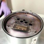
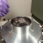
- Place the chips over large holes (rough side down) in the vacuum deposition chamber, depositing aluminum.
- Flip the chips over and repeat again with much smaller holes on the shiny side.
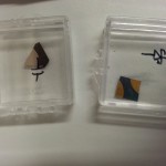
- Completed MOSCAP (left, back side).
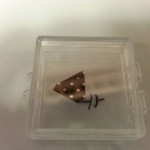
- Completed MOSCAP (front).
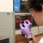
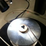
- Place the chip on the analyzer, using the probe to contact one of the aluminum dots.
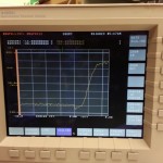
- Graph of the capacitance at various applied voltages.
