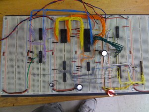
ADC Circuit
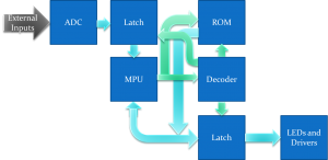
With the initial circuit working well, I now had to add an ADC (analog to digital converter) peripheral. The only additional components needed were the ADC chip and another latch. It could easily be added to the “Final LED Blinking Circuit” by setting the ADC to constantly sample its input and store the result on the latch, and the latch could be connected to the MPU’s data bus (with output depending on the MPU’s address). The flow chart thus was only a bit more complicated.
In fact, the code was a LOT easier than that of the blinking LED, because now I only had to stream input from the ADC latch to the LED latch, and repeat (whereas with the blinking LED, I had to have a timing mechanism).
LATCH = $$0100
ADC	= $$4000
LCD	= $$8000

	    .area MAIN (ABS)
		.org	$$0100

main:	LDAA	ADC
		STAA	LATCH
		BRA 	main
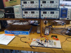
To test the circuit, I set as input to the ADC a signal generator (sine wave), and as output, 8 LEDs to read the digital value of the ADC.
In the following video, you can see the LEDs lighting up in binary according to the voltage on the ADC, which varies as a sine wave. Note how there is no LED activity for a half of each period. That is because the input is half-rectified so the ADC won’t have to deal with negative voltages.
LCD Circuit
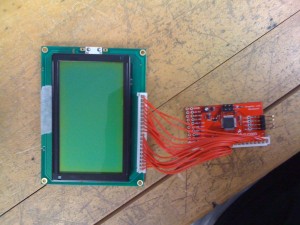
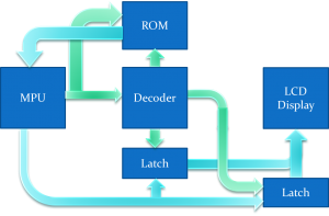
With the initial circuit and ADC tested, I now had to get the LCD working. The LCD would, of course, provide the oscilloscope output. So again, I could simply modify the initial circuit to get the LCD working, except instead of LEDs attached to the latch, I would attach the LCD data pins. Also, the LCD had additional control bits, so that required one more latch.
Unfortunately, I never really got the LCD working properly. The LCD always seemed to display garbage whenever I tried writing to it. Another issue is that we were running out of time, so we had to just go on and put everything together to form the oscilloscope circuit.
