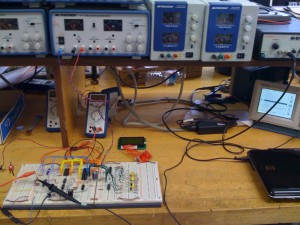
In this semester’s Microprocessor course, I decided to work with a partner to build a complete (and simple) Microprocessor system to serve as an oscilloscope. Unlike many of my other projects involving advanced discrete microcontrollers, this project would utilize the MC6802 MPU (microprocessor unit), which made the electronics aspect of this project a lot harder. In order to get everything working properly, I devised a plan that involved first getting a simple LED blinking circuit working, then adding an ADC component to the circuit, then adding the LCD, and finally coding the oscilloscope. In fact, it turned out to take a while to just get the fundamental circuit to a “complete stage”…
Initial LED Blinking Circuit
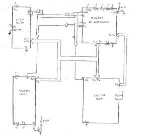
Relatively few parts were needed to complete the “test” circuit.
- MC6802 MPU
- OKI 28C16A ROM
- LS373 Latch
- LS240 Buffer
- Various Logic
The circuit schematic diagram was not too difficult, as well. Actually, one of the hardest parts of wiring was figuring out the correct logic. (The purpose of the logic was to tell certain peripherals when to receive data/send data, and when to remain “quiet”).
Now, while the circuit wiring was somewhat annoying, the actual assembly code needed to run the thing was pretty simple. So simple, in fact, that I started by entering the raw machine code into a hex editor. This wasn’t a really good long term solution, so I asked some others in the class whether they had any suggestions for an assembler. They suggested ASxxxx, which turned out to work quite nicely.
LATCH = $$7FFF
	    .area MAIN (ABS)
	    .org	$$0100

main:	LDAA	#$$00
	    LDS 	#$$007F
m2:	    INCA
	    BSR 	pause
	    STAA	LATCH
	    BRA 	m2

pause:	LDAB	#$$FF
p2:	    DECB
	    BEQ 	p3
	    BRA 	p2
p3:	    RTS
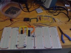
However, while this system wasn’t too hard to set up, there were several major problems. A lot of wiring was required for the logic (despite being such a small test system), and the tri-state buffer method of inserting the start address was too complicated and rigid.
Final LED Blinking Circuit
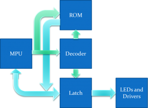
A few generations later, and we arrive at the final blinking LED circuit. The parts involved were:
- MC6802 MPU
- OKI 28C16A ROM
- LS373 Latch
- LS138 Decoder
- Various Logic


